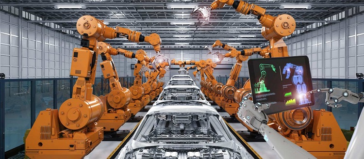
Defect detection plays a crucial role in manufacturing. It ensures efficiency, reduces waste, and maintains product quality. With evolving technologies, the way we detect defects has undergone significant changes. Today, manufacturers can identify issues faster and with greater accuracy, reducing downtime and improving outcomes.
If you are in the manufacturing industry, staying informed about advancements in defect detection is essential. These innovations are transforming quality control, making processes more efficient and cost-effective.
In this article, we will explore key trends shaping the future of defect detection and how they can benefit your business.
Table of Contents
AI-Driven Defect Detection
Artificial Intelligence (AI) has changed how we find problems in manufacturing. Machine learning algorithms can study lots of data. They can find patterns and detect issues with great accuracy. Traditional methods don’t do this. AI systems get better over time. They become more precise with each use.
One big benefit is detecting issues right away. AI-powered sensors and cameras watch the production line. They spot problems as soon as they happen. This cuts delays and stops bad products from getting to customers. It also helps predict maintenance needs. It can find issues before they disrupt work.
Industries like cars and chips already use AI to find defects. For example, in car manufacturing, AI checks engine parts for small cracks that people can’t see. Chip companies also use AI to watch wafer production for flaws. This helps them make high-quality chips.
Patterned Wafers for Semiconductor Defect Detection
Patterned wafers are key in making semiconductors. These wafers help test and improve manufacturing processes. This ensures computer chips have no flaws before full production begins.
Microscopic issues can happen on patterned wafers. So advanced inspection tools are very important. Optical and e-beam systems are often used to find problems. Optical tools check the wafer surface for issues. E-beams look deeper into the microscopic layers.
One popular option is Silyb Patterned Wafers; they are made to fit specific needs. This helps manufacturers work more efficiently and accurately. By matching wafers to the production line, manufacturers can find problems early. They can also optimize processes and reduce waste.
Enhanced defect detection in patterned wafers leads to higher yields. It also lowers production costs. Manufacturers can identify and fix problems during testing. This helps them avoid costly mistakes later on in the process.
The Role of High-Resolution Imaging
High-quality imaging is a big help in finding defects. Today’s cameras and sensors take very detailed pictures. This makes it simpler to spot even tiny flaws.
In some industries, special tools are used to inspect products closely. These tools provide detailed images. They can show problems that might not be seen easily. For example, a camera with high resolution can see scratches, dirt, or issues on the surface of a wafer. This ensures that only perfect products move forward.
The use of advanced imaging systems goes beyond just semiconductors. In electronics, high-quality imaging checks circuit boards for alignment and soldering problems. In textiles, these systems find fabric flaws to ensure consistent quality.
Automated Quality Control Systems
Automation has changed how factories check quality. Automated systems use robots, AI, and cameras to quickly and consistently inspect products.
Robots have advanced sensors. They do precise, repetitive inspections. For instance, when making microchips, robots handle and check patterned wafers. This gives consistent results without human mistakes. Automation speeds up the process. It removes problems caused by tiredness or missing things.
Industries like pharmaceuticals, electronics, and cars use automated systems to find defects. For example, in making medicines, robots check tablets for size and coating. These systems improve accuracy. They also let workers focus on more complex tasks.
Sustainability in Defect Detection
Sustainability is now a top goal for manufacturers. Defect detection helps reach this goal. Advanced defect detection methods find flaws early in production. This cuts waste by catching issues sooner.
For example, wafers must be checked carefully to remove defective materials before being processed. This is important for semiconductor manufacturing. Materials are costly, and any waste will ultimately affect profits.
Eco-friendly defect detection tools can help reach sustainability goals. These include energy-efficient inspection systems. They reduce material use and energy. This lets manufacturers cut their environmental impact while keeping high quality.
Conclusion
Defect detection in manufacturing is changing quickly. New technologies are improving it. AI, high-quality images, patterned wafers, and automated systems are changing quality control. These make it faster, more accurate, and cheaper.
By using these new solutions, factories can produce less waste, work more efficiently, and stay ahead of competitors. Adopt these trends now to make sure your factory is ready for the future.

